


Question
What is the use of AD7 – AD0 in 8085 microprocessor? Explain address de-multiplexing process in 8085 microprocessor with suitable diagram.
AD7 – AD0 in the 8085 microprocessor are the address lines that are used to transfer the memory address to the memory or input/output (I/O) devices. The address lines are 8-bit wide, which allows the 8085 to access up to 256 KB of memory.
Address de-multiplexing in the 8085 microprocessor is the process of separating the address and data signals for efficient transfer of information between the processor and its peripheral devices. The following is the process of address de-multiplexing in the 8085 microprocessor:
- The 8085 microprocessor sends the address and data on the same bus, using the same set of lines.
- A device called the address latch is used to separate the address from the data.
- The address latch is triggered by a control signal called ALE (Address Latch Enable) which is generated by the 8085.
- When ALE goes high, the address latch latches the address onto a separate set of lines and holds it there until the next ALE pulse.
- After the address is latched, the 8085 sends the data on the bus.
- The peripheral device that is addressed by the latched address, reads the data and performs the required operation.
- The address and data signals are multiplexed again for the next cycle, and the process repeats.
The following diagram illustrates the process of address de-multiplexing in the 8085 microprocessor:
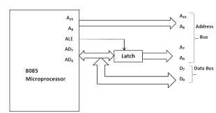
The DE-multiplexed address/data bus allows the 8085 to send both address and data signals in a single cycle, thus increasing the efficiency and speed of the data transfer.